
– Resolution 0.7 nm @ 1 keV, 0.6 nm @ 2-30 keV
– Automatic LoadLock
– CCD IR inspection camera
– Beam deceleration
– Integrated Plasma cleaner
– Oil-free pumping system
– Electron detectors;
-ETD (Everhardt Thornley Detector)
-TLD (Through the Lens Detector)
-MD (Mirror Detector) mounted inside the objective lens; compositional and topographic contrast
-ICD (in-Column Detector) 10 cm above the MD in the column; reduced topographical but highlights compositional contrast
-BSD (Back Scatter Detector) retractable, inserted below the pole piece with 4 different concentric segments
-STEM (Scanning Transmission Electron Microscopy detector) retractable, BF DF HAADF (High Angle Angular Dark Field)
– Energy Dispersive Spectroscopy (EDS) Oxford Xmax 80 mm^2 127eV Silicon Drift Detector
– Electron Backscatter Diffraction (EBSD) detector
- HRSEM- Verios 460L
- HRSEM (including cryo)- Gemini 300, Zeiss
- Plunger- Leica EM GP 2
- S/TEM Spectra 200
- Source:
- X-CFEG: Ultra-high-brightness cold field emission gun with energy resolution of < 0.4 eV.
- Flexible high-tension range from 30 – 200 kV.
- Optical column and corrector:
- Three lens condenser illumination system
- S-CORR probe corrector provides sub-Angstrom imaging resolution at 60 kV as specification and an order of magnitude improvement in optical stability. The S-CORR corrects A5 for all accelerating voltages.
- Symmetric S-TWIN objective lens with widegap pole piece design of 5.4 mm allows double tilt of ± 30° in alfa and beta.
- Resolution:
- Information limit: 110 pm
- STEM resolution: 60 pm @ 200 kV and 136 pm @ 60 kV
- EDS – Super-X detector:
- High-sensitivity, windowless EDS, 4 symmetrical segment detector system based on SDD technology.
- Energy resolution: ≤ 136 eV for Mn-Kα.
- TEM imaging with Ceta-M 16M CMOS camera (with speed enhancement) designed for imaging and diffraction applications.
- STEM imaging with Bright field (BF), Dark field (DF) and/or High Angle Annular Dark Field (HAADF) detectors.
- TEM tomography.
- STEM and EDS tomography.
- iDPC mode (for light elements).
- Precession diffraction with NanoMegas hardware and software package.
- 200 kV
- 60 kV
- Single tilt holder
- Double tilt low background analytical holder (optimized for EDS analysis)
- Double tilt hex-lock analytical holder (for magnetic samples)
- Tomography analytical holder (± 70°)
- NanoEx™–i/v – single tilt TEM holder for heating and biasing
- Sputter coater: Emitech K575X
- Sputter coater: Quorum Q150T ES
The Thermo Fisher Verios 460L field-emission scanning electron microscope (FESEM) offers sub-nanometer resolution over a wide energy range 0.5-30 keV with excellent materials contrast. Its extraordinary low-voltage performance provides extremely precise, surface-specific information even on insulating samples with no conductive coating. The microscope is equipped with a wide array of imaging and analytical detectors for structural and compositional analysis. Verios 460L SEM at the IKI is equipped with an automatic sample loader, and with EDS, EBSD (Oxford Instruments) and STEM detectors.


Gemini 300 field emission scanning electron microscope works both at high vacuum mode and several low vacuum levels. The variable pressure imaging option guarantees maximum versatility enabling in-lens detection in variable pressure (VP) mode. It allows imaging under wide range of accelerating voltages from 0.02 to 30 kV.
It is equipped with the following detectors: the Everhart-Thornley SE detector that collects SE2 electrons and provide topographical information; the high efficiency in-lens detector collects SE1 electrons and provide high resolution surface information; the EsB detector (Energy selective Backscattered) integrated in the Gemini objective lens that collects BS electrons at low voltages and provides low-loss BSE information; the BSD detector (Angular Selective Backscattered) that provides channeling, crystallographic and strain contrasts in addition to compositional or topography information; the VPSE detector (Variable Pressure Secondary Electrons) allowing imaging at low vacuum and the STEM detector collects transmitted electrons of thin samples at several modes (dark field (DF), oriented dark field (ODF), annular dark field (ADF) and high angle annular dark field (HAADF).
The SEM is also equipped with an EDS detector (Bruker XFlash 6, 60mm) and a cryo stage (Leica) for cryo-imaging of soft-materials including biological samples.
Leica EM GP 2 is used for the preparation of vitrified fluid samples or extremely thin samples for cryo-TEM, including biological suspensions and industrial emulsions in both, aqueous and inorganic solvents.

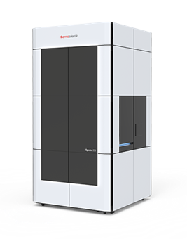
Spectra 200 (S)TEM for Materials Science is a high-throughput platform for atomic-scale materials science investigations. Optimized STEM electron optical performance with probe aberration corrector and ultra-sensitive detection enables the best combination of imaging and analysis. Optimum elemental analysis with EDS provided by the combination of an ultra-high-brightness Cold-FEG (X-CFEG) and Super-X detector configuration to suit the widest range of specimens and experiments. Combination of constant power optics, ultra-high brightness X-CFEG, sensitive detection and the wide-gap pole piece enable to detect light elements (from Boron and above) and most sensitive materials that can be characterized at the atomic scale.
System:
Available techniques:
Available acceleration voltages:
Available holders:
Flash carbon deposition for coating specimens with carbon
Sputter coater for coating specimens with non-oxidising (noble) metals, such as gold, Chromium, platinum, gold- palladium, Nickel and iridium.